ENG-CANSAT-V2-PINOUT
Power Distribution
This section describes the power circuitry used by Cansat V2 and the experiment.
The MCU Board (the Pico) is responsible from its own power regulation.
It can be powered from:
- USB connector: so with 5V. That voltage will be made available on the USB pin.
- VSYS pin : with a voltage from 3 to max 5.5V. A battery can feed that Pin
The MCU board (Pico) can be easily shutdown by placing its 3V3_EN pin to the ground.
Doing so, the Pico 3.3V DC/DC regulator will get deactivated, shutting down the MCU and spare the battery power.
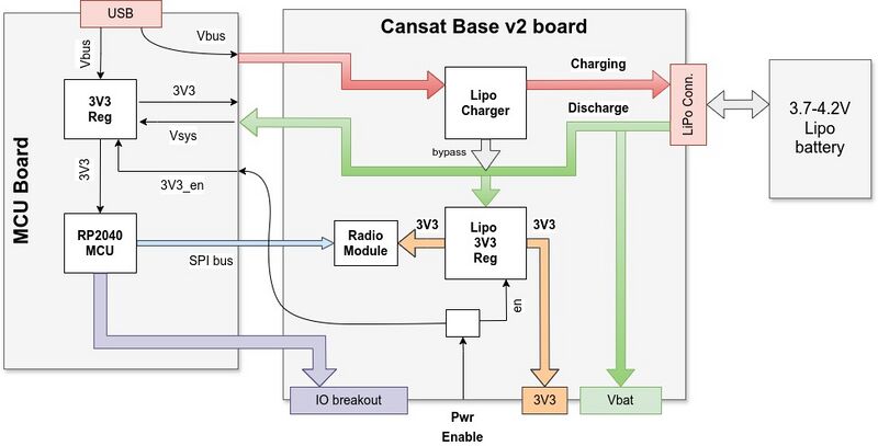
The following diagram show the power distribution circuit with relation between the boards.
Important facts:
- The MCU board is responsible of its own voltage regulation.
- The MCU board regulated voltages are not shared with the Cansat Base board.
- The Cansat Base is responsible of its own voltage regulation.
- The Pwr Enable (on Cansat Base board) disable the voltage regulation on the Cansat Base and MCU board.
When USB plugged on MCU board :
The "MCU board" is powered and generates its 3.3V. VBus is also at 5V and feed the Lipo Charger that charges the Lipo. On the other hand the Lipo being connected, its current voltages (say 4.2V at full charge) feed the Lipo 3V3 Reg and the Vsys on the MCU board. As a result, the "Cansat Base" is also powered with 3.3V (including the radio module).
Remarks:
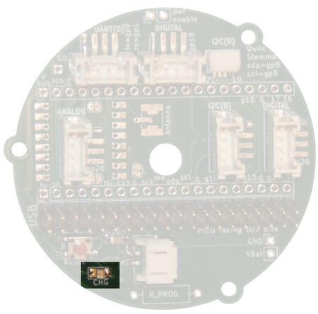
- The CHG charging LED lits while the Lipo is charging.
- The "MCU Board" will be feed either by USB, either by Vsys. The higher voltage path will be used.
- If your Cansat consume as much power as the USB provides to the Lipo then your Lipo will not really charge.
- Close the Pwr Enable pads will shut down the regulators. So all USB Power is used to charge the Lipo.
When USB unplugged :
the Lipo is not charging. The Lipo will discharge into the Lipo 3V3 Reg and MCU board Vsys. The MCU board and Cansat Base are powered.
Remarks:
- Close the Pwr Enable pads will shut down the regulators. This will spare the Lipo Power.
When Lipo is unconnected :
no power can be charged into the Lipo and Lipo cannot get discharged into the voltage regulators. When plugged onto USB the power flow from Vbus to Lipo 3V3 Reg (bypassing the Lipo charger circuitry). So, the Cansat project can be powered from USB for testing purpose.
Remarks:
- The CHG charging LED will continuously blink when Lipo battery is not connected.
- Powering from USB is possible as long as the project is not too power demanding. USB power is limited to 500mA.
When another voltage required :
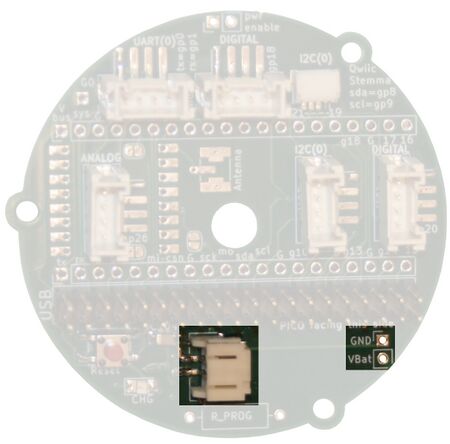
The Vbat pads are available for you to connect a step-up voltage regulator to produce higher voltage from the Lipo battery. Just keep in mind that General Lipo cannot be discharged over 1*C (meaning 1200mAh battery cannot discharge over 1*1200mA before getting the protection activated).
Remarks:
- Cansat must have a minimum weight for the parachute to work efficiently. Having an additional battery may help you to achieve this while offering additional power source for hungry power device (like motor). Just have a common ground between the new battery and existing power circuitry.
Power
Battery
Power Pins
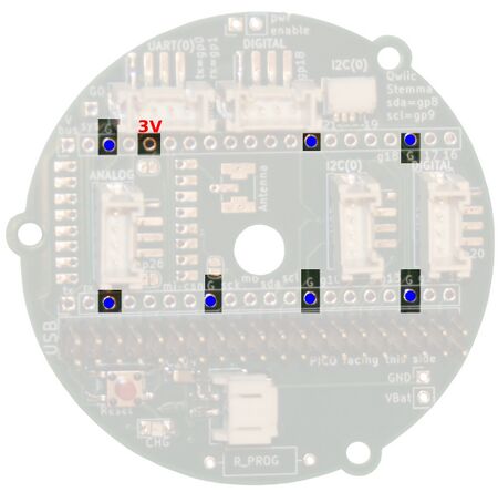
Where to find power on the CANSAT BASE!
|
3V pin is the 3.3V power generated by CANSAT-BASE regulator (nothing regarding with the MCU regulator).
The 3V3 regulator can provide a constant current of 600mA (peak to 1A). Lot of ground GND is made available on the MCU breakout rails (see the Blue points) Voltage is generated either from the Lipo battery or the USB 5V power (see "Power Distribution" here upper).
| ||
|
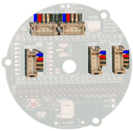
3.3V power is also made available on the Grove connectors and Qwiic/StemmaQt. | ||
|
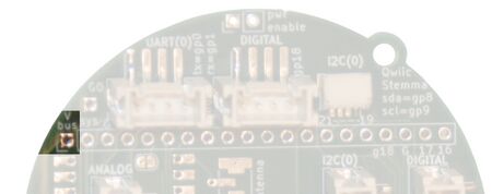
VBus gets 5V (a bit lower) when the MCU board get external power from USB. | ||
|
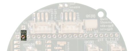
VSys gets Lipo battery voltage (VBat) feeding the MCU board regulator.
Together with VBat pads, Vsys & VBat are the only pins always getting voltage even when the "Power En" shutdown the CANSAT. Think twice before connecting any power consumer device to this pin because it will infinitely drain the power. |
Power Control
|
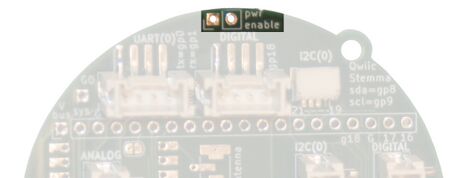
pwr enable signal is keeps high to VBat batch voltage. It keeps the voltage regulators actives of the CANSAT-BASE and the MCU-Board. Tie this signal to ground to disable the voltage regulators on both board.
The convenient place of the pwr enable pads allows you to control this feature with just a piece of wire to connect the both pads together. It is also possible to mount a switch or a jumper on the pads. | ||
|
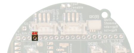
en signal controls the voltage regulator of the MCU board. It is maintain high to VSYS on the MCU board. When set LOW, the MCU voltage regulator get disabled.
|
Radio Module
The radio module is powered with 3V regulator of the CANSAT-BASE.
The radio module is controled via a SPI bus and a dedicated Reset line.
|
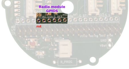
Some of the GPIOs are attached to radio module.
As a consequence they are not available for use on the GPIO breakout.
| ||||||||||||||||||
|
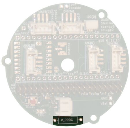
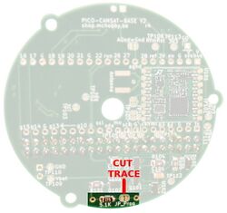
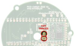
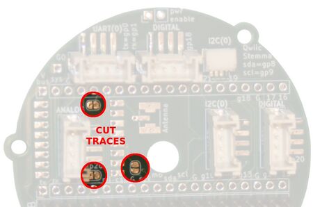
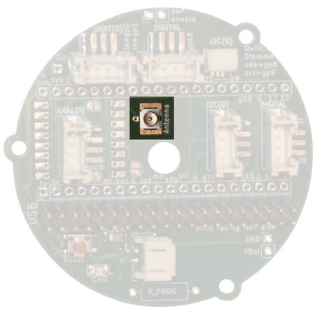
It is possible to deactivate the radio module and release the attached GPIOs.
Cut the 5 jumper traces highlighted in the two following picture. | ||||||||||||||||||
|
The uFl/IPX connector is used to connect the external antenna. |
Connectors
The CANSAT-BASE features many GROVE connectors and a Qwiic/StemmaQt connector.
They can be used to make the connections easy.
I2C connectors
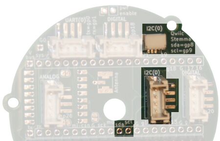
Among all the connections, the most important are the sda & scl signal attached to the I2C bus.
The SDA (Serial Data) and SCL (Serial Clock) are used to ship back and forward the data from one of the device connected on the I2C bus.
I2C devices/sensors can be daisy chained on the same bus since each device having an unique I2C address (7 bits address, value from 1 to 127).
Such way, the microcontroler can get in touch with a given sensor over the I2C bus to send configuration data and query measurement results.
|
Two GPIOs are attached to the board I2C module.
The I2C is accessible via any (or all) of:
|
UART connector
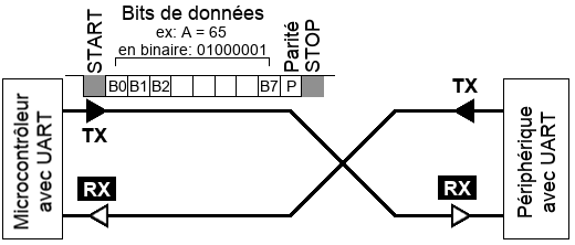
The UART is often called serial line, it is a bidirectional communication bus used to communicate with an UART device. Most common device are GPS, Mobile Phone Chips, WiFi/Bluetooth chips.
The UART also use two signals:
- The TX (transmission) line from the microcontroler is connected to the RX line on the GPS.
- The RX (reception) line on the microcontroler is feed with the TX line of the GPS.
Before exchanging data, both device must be initialized with the same device configuration (communication speed in bauds, number of bits, parity and number of stop bits).
A common configuration is 9600 bauds, 8 bits Data, NO parity, 1 stop bit usually summarize as "9600 8N1". The next most common configuration is "115200 8N1".
When a device sends data, the uart will decompose the data into a sequence of bits (sequence of 1 and 0) THEN emit the bits one by one over the serial line.
As the both devices agreed on the communication parameter, the receiver can properly interpret the bits sequences TO recompose the original data.

|
Two GPIOs are attached to the board I2C module.
The UART(0) is accessible via any (or all) of:
|
PinOut summary
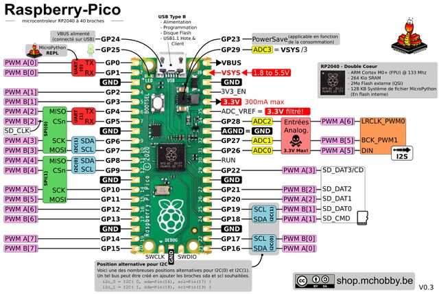
The "CANSAT-BASE Breakout" column refer to the CANSAT-BASE Breakout row (which is also the same identification on a Pico GPIO).
The "Reserved Usage" column is YES when the pin is dedicated to a specific usage (EG: Radio module, Voltage Reference).
The "Function" column is specified only when usage of the pin usage is restricted.
| CANSAT-BASE Breakout |
Reserved Usage |
Function | Description |
| gp0 | no | uart.tx | UART(0) Grove connector |
| gp1 | no | UART.rx | UART(0) Grove connector |
| gp2 | no | ||
| gp3 | YES | IO | Radio module reset line (can be released) |
| gp4 | YES | SPI.miso | Radio module (can be released) |
| gp5 | YES | SPI.nss | Radio module select line (can be released) |
| gp6 | YES | SPI.sck | Radio module clock line (can be released) |
| gp7 | YES | SPI.mosi | Radio module (can be released) |
| gp8 | YES | I2C.sda | I2C(0) Grove connector, I2C(0) Qwiic/StemmaQt connector. |
| gp9 | YES | I2C.scl | I2C(0) Grove connector, I2C(0) Qwiic/StemmaQt connector. |
| gp10 | no | ||
| gp11 | no | ||
| gp12 | no | ||
| gp13 | no | ||
| gp14 | no | ||
| gp15 | no |
| CANSAT-BASE Breakout |
Reserved Usage |
Function | Description |
| gp16 | no | ||
| gp17 | no | ||
| gp18 | no | Digital | Digital1 Grove connector |
| gp19 | no | Digital | Digital1 Grove connector |
| gp20 | no | Digital | Digital2 Grove connector |
| gp21 | no | Digital | Digital2 Grove connector |
| gp22 | no | ||
| run | YES | Reset | Reset button. Set LOW to reset. |
| gp26 | no | Analog IN | Analog Grove Connector |
| gp27 | no | Analog IN | Analog Grove Connector |
| agnd | YES | Analog Ground | |
| gp28 | no | ||
| ref | YES | MCU VRef | Voltage Reference of the MCU Board (usually unconnected). |
| 3V3 | YES | Power-OUT | CANSAT-BASE 3V3 Voltage Output. Unrelated to MCU board voltage regulator |
| en | YES | 3V3_en | MCU Voltage Regulator enable. Set to ground to disable MCU. Controled by the CANSAT-BASE pwr_enabled. |
| sys | YES | MCU Power-IN | MCU Vsys. MCU System Voltage used by the MCU to produces its internal voltages. |
| Vbus | YES | USB Power-OUT | Voltage output when power is applied to the MCU's USB connector |
Written by Meurisse D. for MCHobby
