Différences entre versions de « Spark-Photon-Brochage »
| Ligne 182 : | Ligne 182 : | ||
| I/O pin capacitance ||CIO ||||||5 ||||pF | | I/O pin capacitance ||CIO ||||||5 ||||pF | ||
|} | |} | ||
| + | |||
| + | {{underline|Notes:}} | ||
| + | |||
| + | [1] FT = Five-volt tolerant. In order to sustain a voltage higher than V3V3+0.3 the internal pull-up/pull-down resistors must be disabled. | ||
| + | |||
| + | [2] Hysteresis voltage between Schmitt trigger switching levels. Based on characterization, not tested in production. | ||
| + | |||
| + | [3] With a minimum of 100mV. | ||
| + | |||
| + | [4] Leakage could be higher than max. if negative current is injected on adjacent pins. | ||
| + | |||
| + | [5] Pull-up and pull-down resistors are designed with a true resistance in series with switchable PMOS/NMOS. This PMOS/NMOS contribution to the series resistance is minimum (~10% order). | ||
{{Spark-Photon-Materiel-TRAILER}} | {{Spark-Photon-Materiel-TRAILER}} | ||
Version du 2 juillet 2015 à 20:53
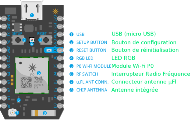
Brochage

Crédit: Particle.IO www.particle.io
| Pin | Description |
| VIN |
This pin can be used as an input or output. As an input, supply 3.6 to 5.5VDC to power the Photon. When the Photon is powered via the USB port, this pin will output a voltage of approximately 4.8VDC due to a reverse polarity protection series schottky diode between VUSB and VIN. When used as an output, the max load on VIN is 1A. |
| RST |
Active-low reset input. On-board circuitry contains a 1k ohm pull-up resistor between RST and 3V3, and 0.1uF capacitor between RST and GND. |
| VBAT | Supply to the internal RTC, backup registers and SRAM when 3V3 is not present (1.65 to 3.6VDC). |
| 3V3 | This pin is the output of the on-board regulator and is internally connected to the VDD of the WiFi module. When powering the Photon via VIN or the USB port, this pin will output a voltage of 3.3VDC. This pin can also be used to power the Photon directly (max input 3.3VDC). When used as an output, the max load on 3V3 is 100mA. NOTE: When powering the Photon via this pin, ensure power is disconnected from VIN and USB. |
| WKP | Active-high wakeup pin, wakes the module from sleep/standby modes. When not used as a WAKEUP, this pin can also be used as a digital GPIO, ADC input or PWM. |
| D0~D7 | Digital only GPIO pins. |
| A0~A9 | 12-bit Analog-to-Digital (A/D) inputs (0-4095), and also digital GPIOs. A6 and A7 are code convenience mappings, which means pins are not actually labeled as such but you may use code like analogRead(A7). A6 maps to the DAC pin and A7 maps to the WKP pin. |
| DAC | 12-bit Digital-to-Analog (D/A) output (0-4095), and also a digital GPIO. DAC is used as DAC1 in software, and A5 is a second DAC output used as DAC2 in software. |
| RX | Primarily used as UART RX, but can also be used as a digital GPIO or PWM. |
| TX | Primarily used as UART TX, but can also be used as a digital GPIO or PWM. |
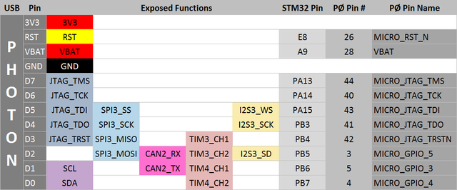
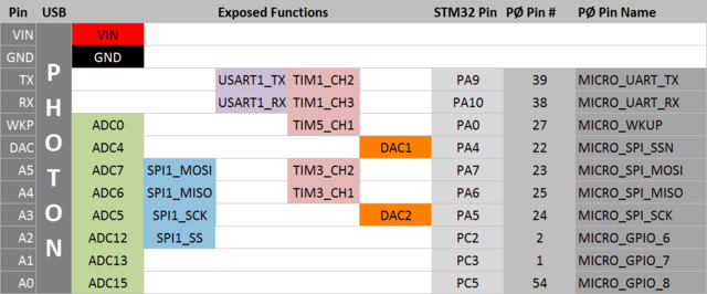
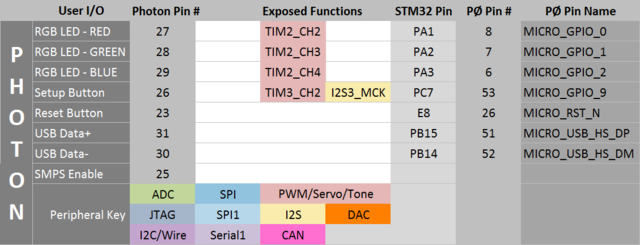
Diagramme des broches

Crédit: Particle.IO www.particle.io

Crédit: Particle.IO www.particle.io

Crédit: Particle.IO www.particle.io
Spécifications techniques
Valeurs maximales absolues
| Parameter | Symbol | Min | Typ | Max | Unit |
| Supply Input Voltage | VIN-MAX | +6.5 | V | ||
| Supply Output Current | IIN-MAX-L | 1 | A | ||
| Supply Output Current | I3V3-MAX-L | 100 | mA | ||
| Storage Temperature | Tstg | -40 | +85 | °C | |
| Enable Voltage | VEN | VIN+0.6 | V | ||
| ESD Susceptibility HBM (Human Body Mode) | VESD | 2 | kV |
Conditions de fonctionnement recommandées
| Parameter | Symbol | Min | Typ | Max | Unit |
| Supply Input Voltage | VIN | +3.6 | +5.5 | V | |
| Supply Input Voltage | V3V3 | +3.0 | +3.3 | +3.6 | V |
| Supply Output Voltage | VIN | +4.8 | V | ||
| Supply Output Voltage | V3V3 | +3.3 | V | ||
| Supply Input Voltage | VVBAT | +1.65 | +3.6 | V | |
| Supply Input Current (VBAT) | IVBAT | 19 | uA | ||
| Operating Current (Wi-Fi on) | IIN avg | 80 | 100 | mA | |
| Operating Current (Wi-Fi on) | IIN pk | 235[1] | 430[1] | mA | |
| Operating Current (Wi-Fi on, w/powersave) | IIN avg | 18 | 100[2] | mA | |
| Operating Current (Wi-Fi off) | IIN avg | 30 | 40 | mA | |
| Sleep Current (5V @ VIN) | IQs | 1 | 2 | mA | |
| Deep Sleep Current (5V @ VIN) | IQds | 80 | 100 | uA | |
| Operating Temperature | Top | -20 | +60 | °C | |
| Humidity Range Non condensing, relative humidity | 95 | % |
Notes:
[1] These numbers represent the extreme range of short peak current bursts when transmitting and receiving in 802.11b/g/n modes at different power levels. Average TX current consumption in will be 80-100mA.
[2] These are very short average current bursts when transmitting and receiving. On average if minimizing frequency of TX/RX events, current consumption in powersave mode will be 18mA
Spécifications WiFi
| Feature | Description |
| WLAN Standards | IEEE 802 11b/g/n |
| Antenna Port | Single Antenna |
| Frequency Band | 2.400 GHz – 2.484 GHz |
| Sub Channels | 1 ~ 14 |
| Modulation | DSSS, CCK, OFDM, BPSK, QPSK,16QAM, 64QAM |
| PØ module Wi-Fi output power | ' | Typ. | Tol. | Unit |
| RF Average Output Power, 802.11b CCK Mode | 1M | 16.5 | +/- 1.5 | dBm |
| 11M | 16.5 | +/- 1.5 | dBm | |
| RF Average Output Power, 802.11g OFDM Mode | 6M | 15 | +/- 1.5 | dBm |
| 54M | 13 | +/- 1.5 | dBm | |
| RF Average Output Power, 802.11n OFDM Mode | MCS0 | 14.5 | +/- 1.5 | dBm |
| MCS7 | 12 | +/- 1.5 | dBm |
Caractéristiques I/O
These specifications are based on the STM32F205RG datasheet, with reference to Photon pin nomenclature.
| Parameter | Symbol | Conditions | Min | Typ | Max | Unit |
| Standard I/O input low level voltage | VIL | -0.3 | 0.28*(V3V3-2)+0.8 | V | ||
| I/O FT[1] input low level voltage | VIL | -0.3 | 0.32*(V3V3-2)+0.75 | V | ||
| Standard I/O input high level voltage | VIH | 0.41*(V3V3-2)+1.3 | V3V3+0.3 | V | ||
| I/O FT[1] input high level voltage | VIH | V3V3 > 2V | 0.42*(V3V3-2)+1 | 5.5 | V | |
| VIH | V3V3 ≤ 2V | 0.42*(V3V3-2)+1 | 5.2 | V | ||
| Standard I/O Schmitt trigger voltage hysteresis[2] | Vhys | 200 | mV | |||
| I/O FT Schmitt trigger voltage hysteresis[2] | Vhys | 5% V3V3[3] | mV | |||
| Input leakage current[4] | Ilkg | GND ≤ Vio ≤ V3V3 GPIOs | ±1 | µA | ||
| Input leakage current[4] | Ilkg | RPU | Vio = 5V, I/O FT | 3 | µA | |
| Weak pull-up equivalent resistor[5] | RPU | Vio = GND | 30 | 40 | 50 | k Ω |
| Weak pull-down equivalent resistor[5] | RPD | Vio = V3V3 | 30 | 40 | 50 | k Ω |
| I/O pin capacitance | CIO | 5 | pF |
Notes:
[1] FT = Five-volt tolerant. In order to sustain a voltage higher than V3V3+0.3 the internal pull-up/pull-down resistors must be disabled.
[2] Hysteresis voltage between Schmitt trigger switching levels. Based on characterization, not tested in production.
[3] With a minimum of 100mV.
[4] Leakage could be higher than max. if negative current is injected on adjacent pins.
[5] Pull-up and pull-down resistors are designed with a true resistance in series with switchable PMOS/NMOS. This PMOS/NMOS contribution to the series resistance is minimum (~10% order).
Source: Particle Photon Hardware créé par Particle.IO.
Traduction réalisée par Meurisse D pour MCHobby.be - Translated by Meurisse D. for MCHobby.be
Traduit avec l'autorisation de Particle.IO - Translated with the permission from Particle.IO - Particle.IO
Toute référence, mention ou extrait de cette traduction doit être explicitement accompagné du texte suivant : « Traduction par MCHobby (www.MCHobby.be) - Vente de kit et composants » avec un lien vers la source (donc cette page) et ce quelque soit le média utilisé.
L'utilisation commercial de la traduction (texte) et/ou réalisation, même partielle, pourrait être soumis à redevance. Dans tous les cas de figures, vous devez également obtenir l'accord du(des) détenteur initial des droits. Celui de MC Hobby s'arrêtant au travail de traduction proprement dit.